74LCX16652 Overview
Key Specifications
Package: TSSOP
Mount Type: Surface Mount
Pins: 56
Operating Voltage: 2.5 V
Description
The LCX16652 contains sixteen non-inverting bidirectional bus transceivers with 3-STATE outputs providing multiplexed transmission of data directly from the input bus or from the internal registers. Data on the A or B bus will be clocked into the registers as the appropriate clock pin goes to the HIGH logic level.
Key Features
- Specify by appending the suffix letter “X” to the ordering code
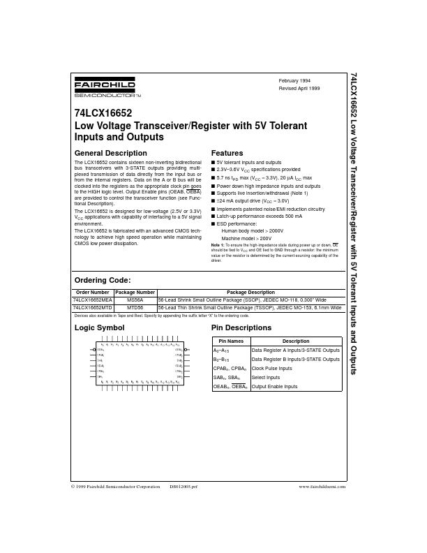
- Logic Symbol Pin Descriptions Pin Names A0–A15 B0–B15 CPABn, CPBAn SABn